
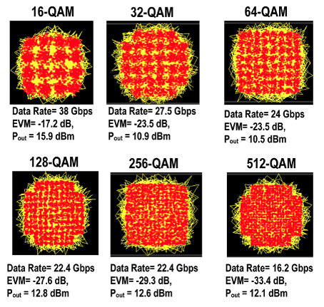
Research Projects
Five interconnected research thrusts advancing the frontiers of mm-wave, THz, and AI-driven electronics.
Research in Detail
Explore each of our five research thrusts, from fundamental device physics to AI-powered circuit design.
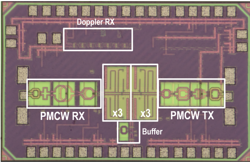
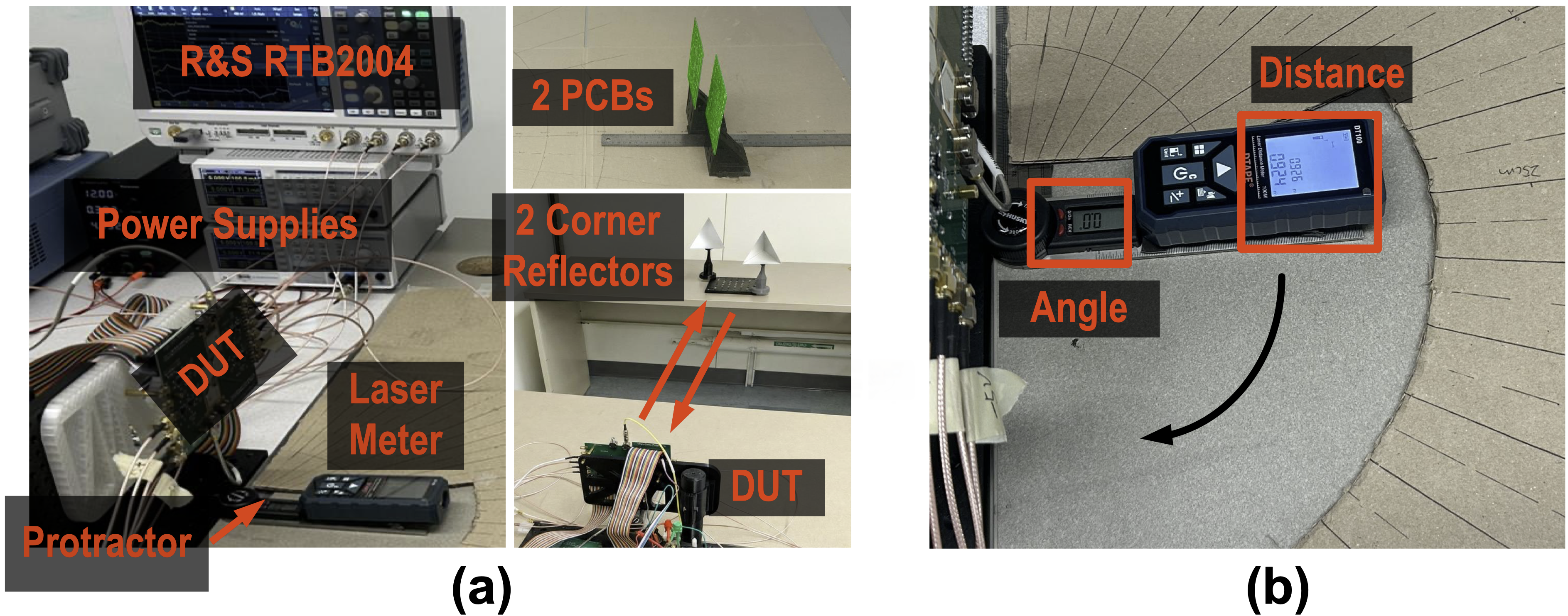
Multi-Band Millimeter-Wave Radars
Phase-frequency-locked mm-wave radar for sensing and imaging
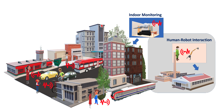
The internet-driven communication networks revolutionized human access to information during the past three decades. Building on advances in communication, security, and sensing technologies, cyber-physical systems are now poised to transform machine-to-machine and human-to-machine interactions. Realization of local-area sensing networks for such infrastructures requires tight integration of sensing, computation, control, and networking within physical entities. Emerging applications—such as high-precision vital signs monitoring, human-robot interaction, chemical sensing, and 3D defect detection—demand massive networks of portable miniaturized sensors capable of resolving range, angular, and cross-range dimensions with high fidelity.
To address these challenges, our research explores multi-band, phase–frequency-locked millimeter-wave radars that combine wideband operation with precise frequency synthesis and phase coherence across multiple sub-bands. These scalable radar front-ends enable fine-resolution 3D imaging and adaptive sensing across centimeter-to-meter ranges while maintaining compactness and energy efficiency. In parallel, we investigate new classes of wideband active sensors and emerging device technologies that together form the foundation of intelligent, low-power sensing architectures for next-generation cyber-physical systems.
Applications
Related Publications
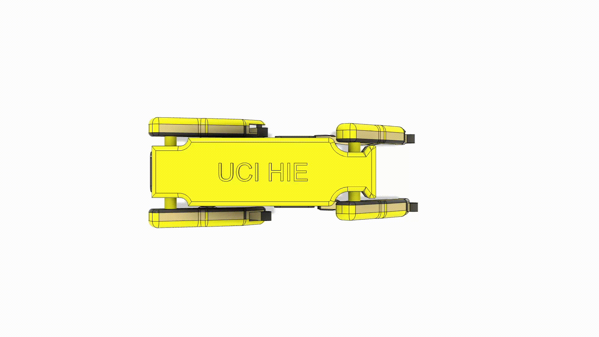
Gallery

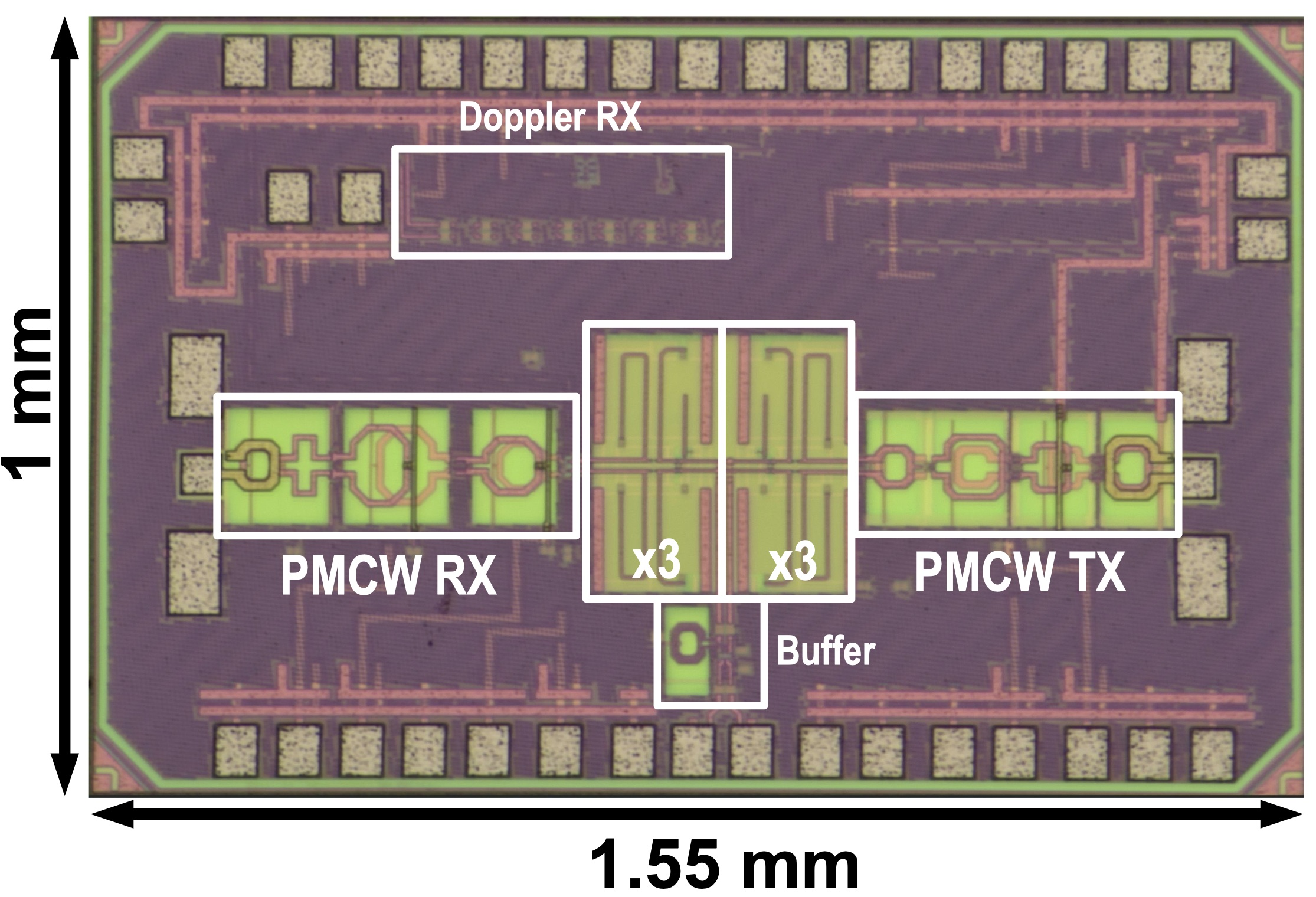
Sub-THz and THz Efficient Power Generation
Signal generation beyond transistor frequency limits
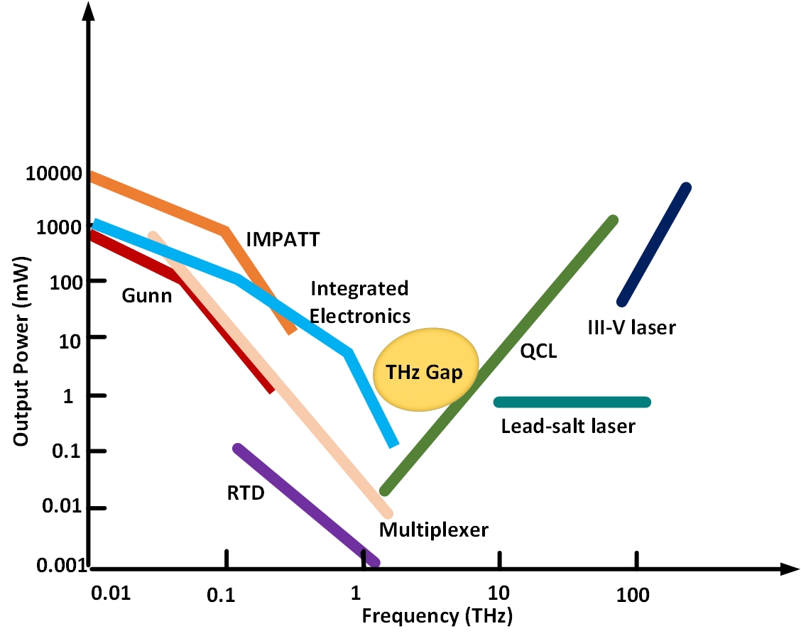
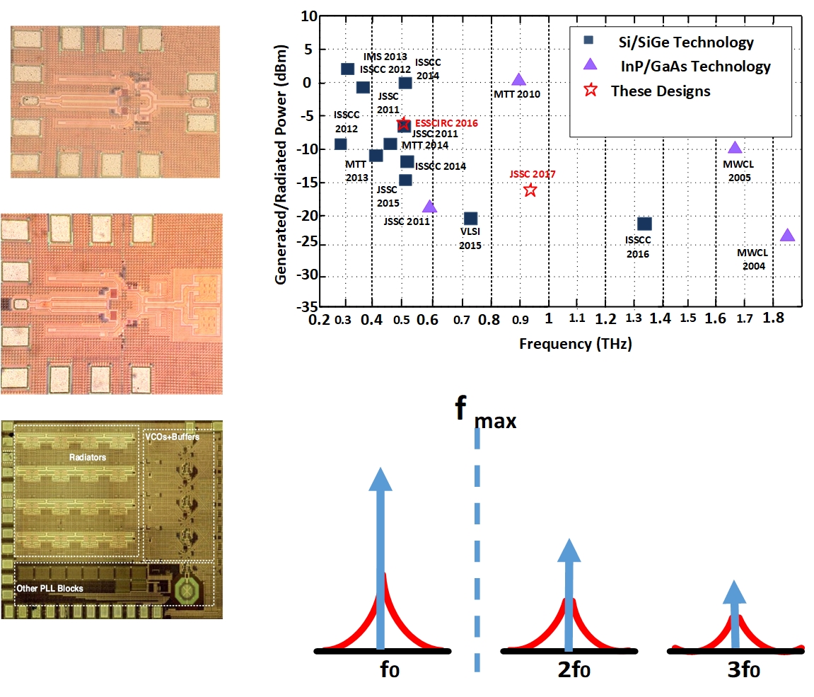
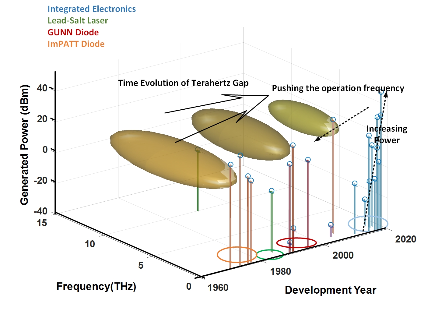
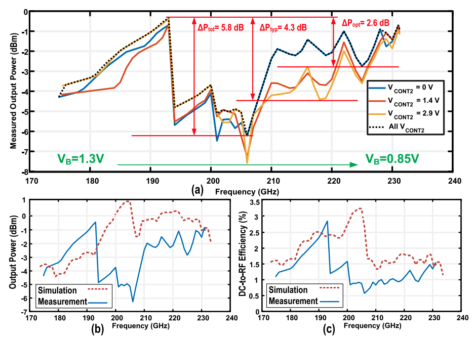
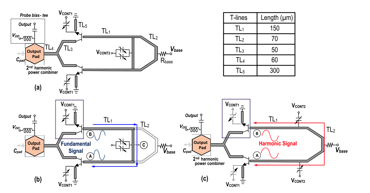
There are growing applications in the mm-wave and sub-mm-wave frequency ranges due to smaller wavelengths compared to radio frequencies, plethora of water-absorption bands, and larger available bandwidth of data transmission. Integrated solutions have become the desired platforms to realize systems at these frequencies thanks to their high yield and low cost. Signal generation beyond the fmax of transistors, relies on the generation of high power harmonic signals. Due to the limited efficiency of harmonic signals, high power generation remains a challenge.
By finding the major nonlinear mechanisms of power generation in transistors, we propose a large-signal model and a design methodology based on the Volterra-Weiner theory to optimize the desired nonlinear behavior of a transistor or of any nonlinear element. The combination of arbitrary passive networks and the nonlinear element are formulated to find the optimum circuit configuration to achieve desired performance. The proposed systematic model extraction, which is not limited to any particular transistor type, can be exploited to capture the nonlinear behavior of MOSFET, BJT, HBT, HEMT, MESFET, HFET, or other transistor types.
Applications
Related Publications
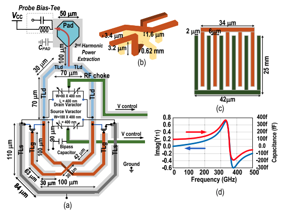
Gallery
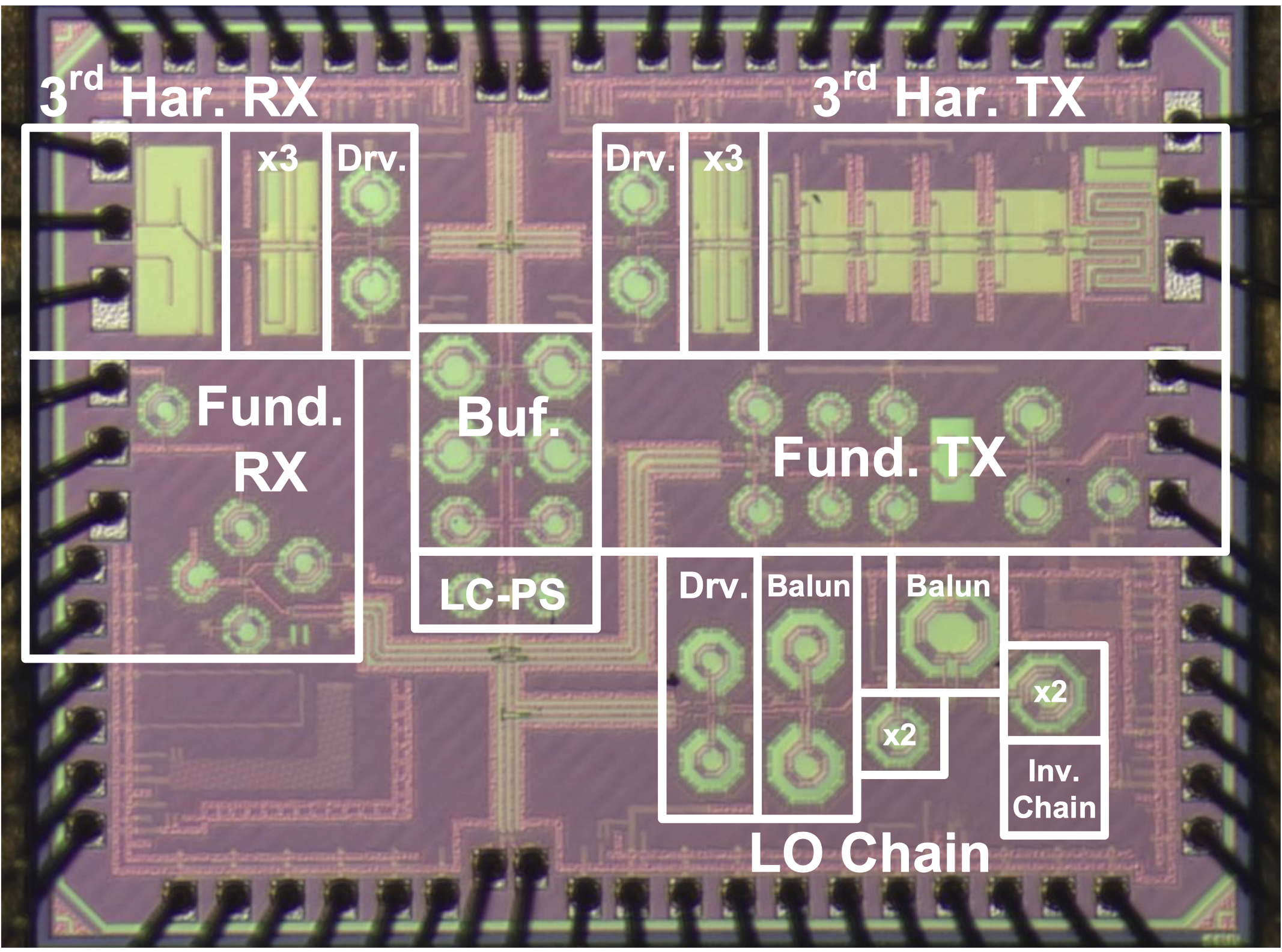
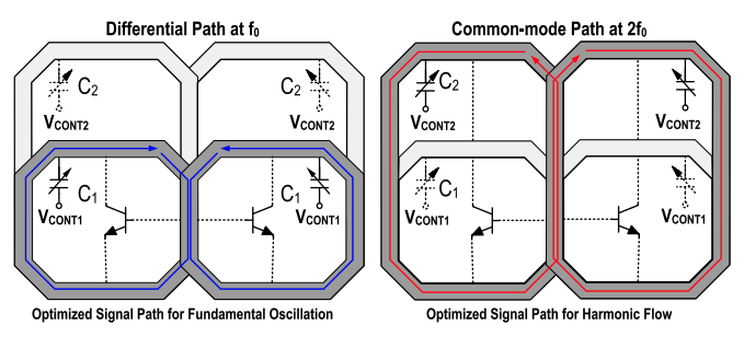
Efficient Wideband and Low Phase Noise Signal Generation at mm-wave Frequencies
Novel oscillator structures for mm-wave and THz applications
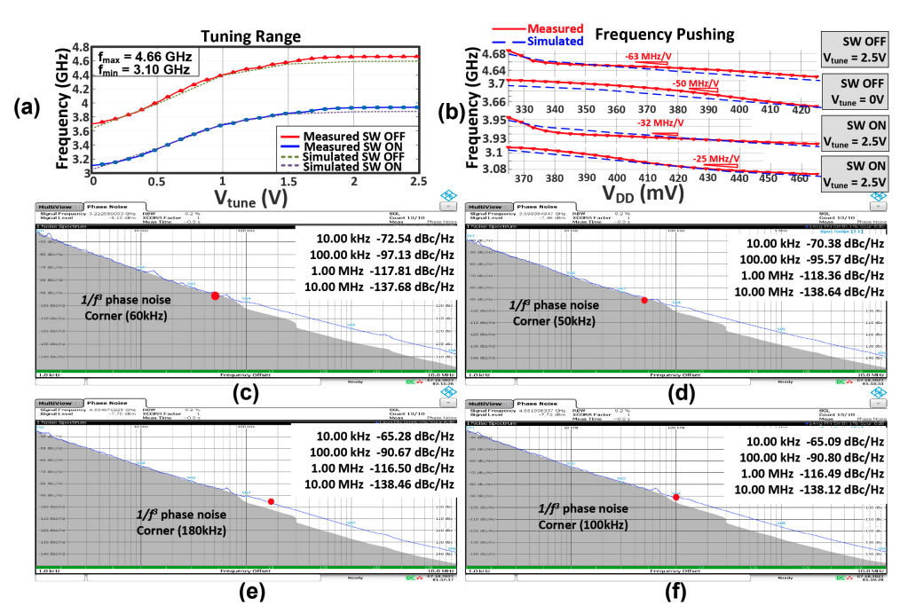
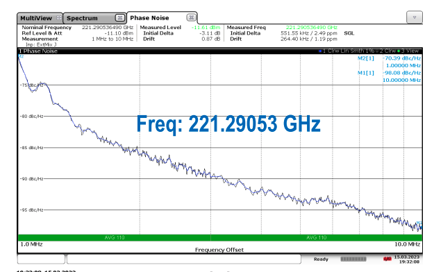
One of the challenges of signal generation at high frequency is the degradation of oscillatory waveform in terms of purity and tuning capability. The loss associated with passive components increase by going to mm-wave and terahertz frequencies which directly impacts the phase-noise of the oscillators. On the other hand, the tuning components such as varactors need to exhibit both a high quality factor and a large variation of the capacitance which is not feasible as they become comparable with the device parasitic capacitors.
By implementing novel oscillator structures which resolve the phase-noise and tuning-range limitation of mm-wave and terahertz oscillators, emerging applications such as high frequency communication circuits, sensing, and imaging are enabled.
Applications
Related Publications
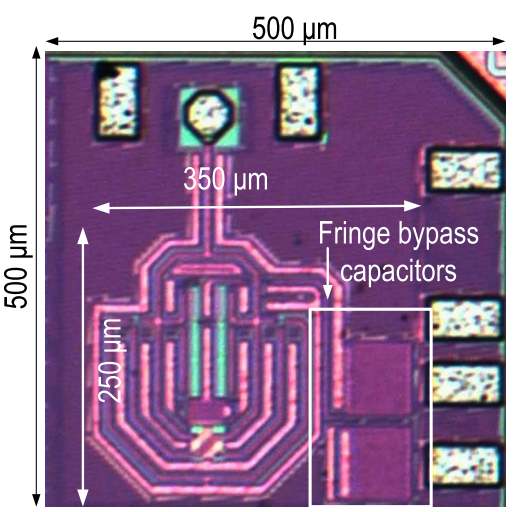
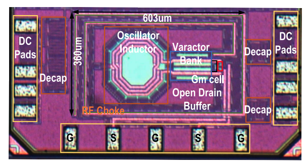
Gallery
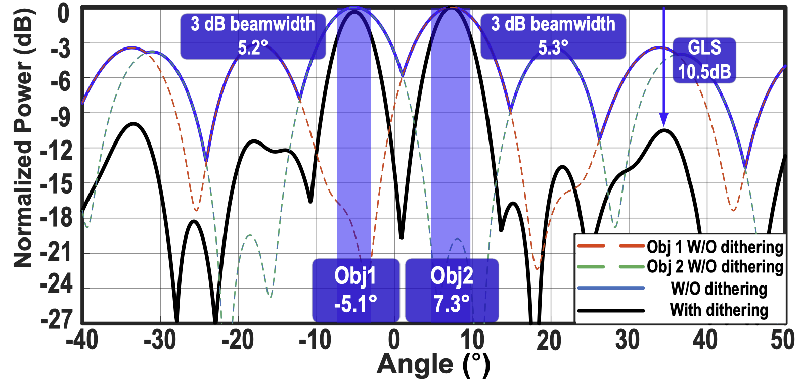
AI-Driven Analog/RF Design and Sensing Systems
Machine learning meets circuit synthesis and radar sensing
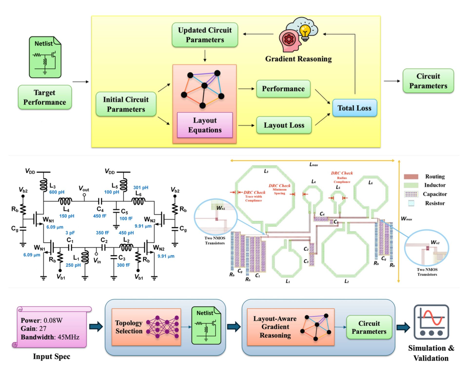
Artificial intelligence is used both to design analog/RF systems and to operate sensing front-ends efficiently. On the design side, we develop a layout-aware ML pipeline that links specification → topology → sized circuit with physical constraints, using graph-based predictors and inverse design to generate DRC-compliant solutions that account for post-layout parasitics.
On the sensing side, we build attention-guided beam control that prioritizes regions of interest for FMCW/reflectarray radars, adaptively steering direction and beamwidth to reduce redundant scans while preserving angular resolution. Unifying these threads, AI acts as an end-to-end enabler—from rapid design-space exploration and layout-constrained synthesis to closed-loop beam adaptation in deployment—improving turnaround time, robustness to process/layout variation, and scene-aware sensing performance across mm-wave and sub-THz regimes.
Applications
Related Publications
Gallery

Emerging Device Technologies
All-spin-logic and Janus 2D material devices
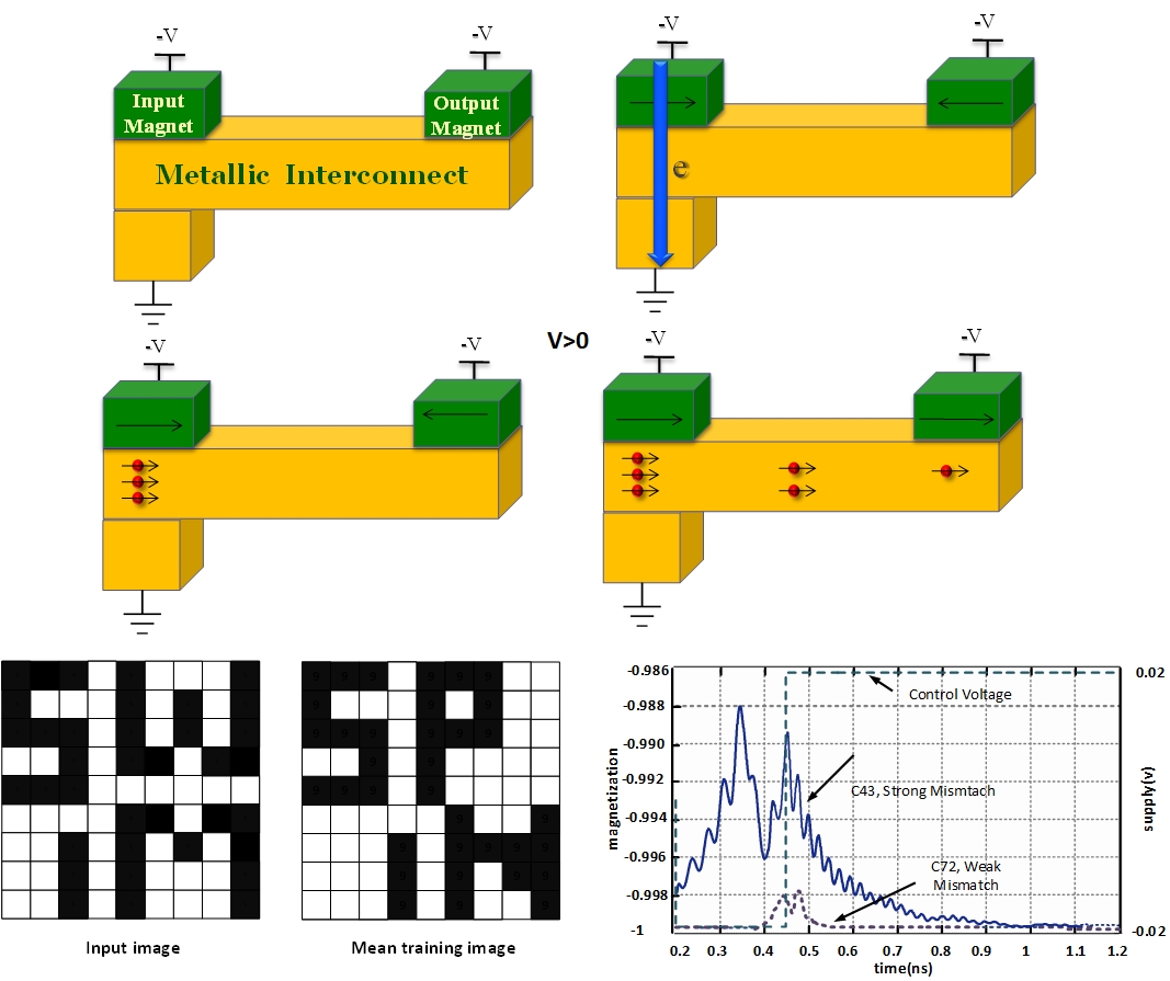
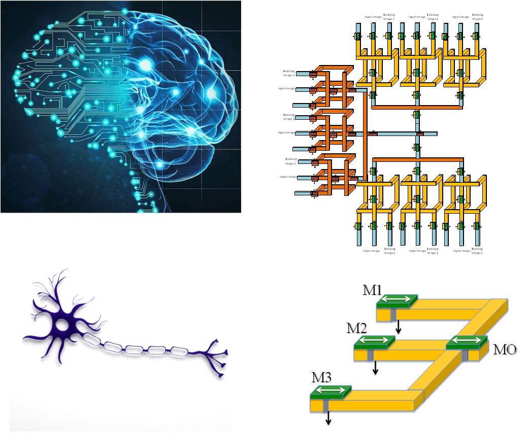
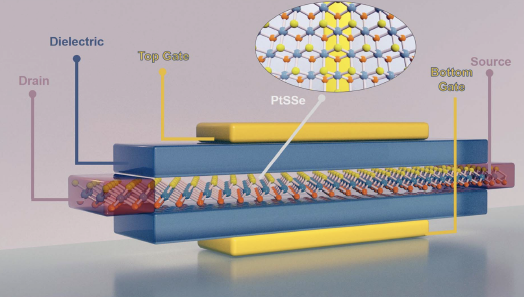
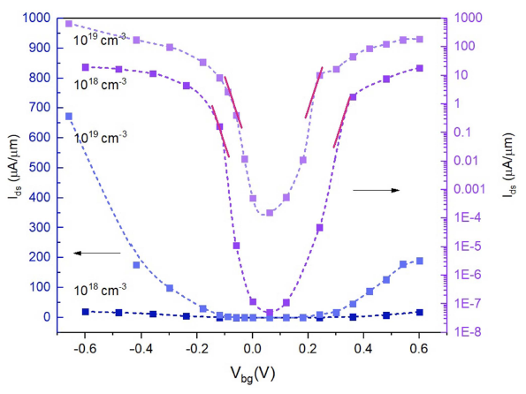
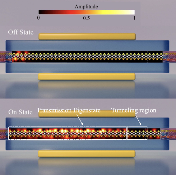
Our research targets viable alternatives to CMOS for next-generation computing and ultra-low-power operation by advancing two complementary device frontiers: (i) all-spin-logic “smart detector cells” that tightly merge memory and computation to enable non-Boolean pattern recognition with instant-on behavior and microwatt-class power, and (ii) steep-slope tunneling FETs built on Janus 2D materials (PtSSe) that demonstrate sub-60 mV/dec switching, Ion/Ioff >10⁸, and THz-scale operating speed—together pointing to energy-aware, compact architectures that leverage spin transport, quantum tunneling, and atomically engineered channels to move beyond CMOS.
Applications
Related Publications
Gallery
Interested in Collaboration?
We welcome research collaborations from academia and industry. If our work aligns with your interests, let's connect.